HARTING recognized the need for a solution as many applications require a lot of manual work, which is inefficient and error-prone. A comprehensive analysis of manual work steps in PCB assemblies revealed that a large percentage of them are due to the vertical assembly of one or more electronic components to the main PCB. HARTING engineers have taken up the challenge of developing a component that will increase automation, save work steps, and reduce costs for customers. Result: The 3D-MID Component Carrier.
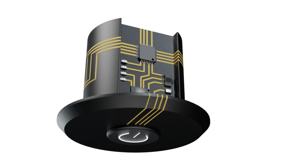
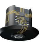
3D-MID also known as 3D-Circuits, stands for “3D Mechatronic Integrated Device,” a manufacturing technology in which circuits are integrated directly into three-dimensional plastic parts.
Versatile solution for various challenges
HARTING knows that integrating more functions in limited space and driving miniaturization are critical aspects in the development of medical products. The 3D-Circuits Component Carrier addresses these pain points efficiently.
1. Vertical Placement of Electronic Components
Vertical placement of electronic components on a PCB is challenging because it usually requires manual assembly. This can be time-consuming, labor-intensive and lead to errors.
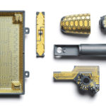
HARTING’s Chip Carrier is a solution that addresses these challenges. It is suitable for a wide range of applications, including Hall effect and acceleration sensors, ICs, and LED applications. It is also compatible with multiple soldering processes, making it a versatile and flexible solution.
Here are some of the key benefits of the Chip Carrier:
- Eliminates the need for manual assembly
- Improves accuracy and repeatability
- Compatible with multiple soldering processes
- Versatile and variable
The assembled component carrier can be fully automated as a sub-assembly on standard SMT machines. This simplifies the production process and offers the potential to miniaturize your final product.
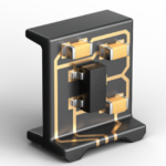
2. Eliminating piggyback boards
Piggyback PCBs are two separate PCBs that are stacked on top of each other. They are often used when there is not enough space for a single PCB. 3D-Circuits offer a number of benefits over piggyback PCBs. They are smaller, lighter, and easier to manufacture. They also offer greater design flexibility and can be processed fully automatically with SMT machines.
As a result, 3D circuits are becoming increasingly popular in a variety of applications in medical, automotive as well as in industrial and consumer electronics. The Chip Carrier is a valuable solution for anyone who is looking to simplify the vertical placement of electronic components on PCBs. It is a time-saving, cost-effective, and reliable solution that can be used in a wide range of applications.
3. Adapter function
The HARTING component carrier can be used as an adapter for alternative packaging. This is particularly useful if your original component is no longer available, but you want to use another component with the same function.
The component carrier adapts the footprint of the alternative package to the footprint of the original component. There is no need to change the layout of the main PCB and this means validation and qualification loops can be avoided, this saves time and money.
Additional benefit: With the highly fluctuating delivery times of semiconductors, security of supply is further increased in this way.

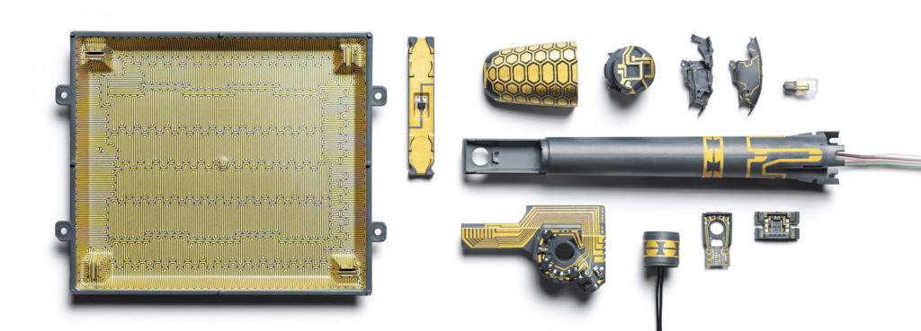
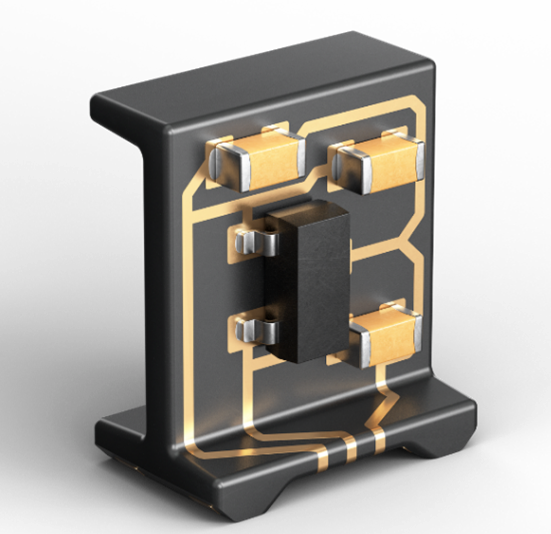
3D-Circuit layout design and manufacturing of component carrier
Altium offers exciting capabilities for PCB layouts with the new 3D Circuit Design. Engineers can import the chip carrier 3D file into Altium Designer and perform routing individually on the carrier’s surface. The exported design can be directly used for customized manufacturing of a component carrier.
On the injection-molded substrate of the carrier, a laser ablates a thin layer of the thermoplastic, creating a pattern that is used in the subsequent chemical plating process to build-up electrical conductors. In this way, customized layouts and designs can be created with easy adaptation of the laser program.
The electronic components are assembled by HARTING. In the process, the components are also glued to the chip carrier to withstand subsequent soldering processes several times without the components shifting.
Conclusion
HARTING’s 3D circuit carrier is based on a proven technology with a track record of success. It was introduced at HARTING in 2003 and has been used in a variety of automotive and medical applications.
HARTING has the complete process chain in-house, from initial design to final production. This gives HARTING complete control over the quality, cost, and delivery of products.
HARTING works closely with customers to develop the best possible component carrier design. If the layout cannot be added to an existing injection-molded part, HARTING can also create customized solutions.