3D-MID is the abbreviation for “Three-dimensional Mechatronic Integrated Devices”. Mechatronics is a term coined by the Japanese company Yaskawa in 1969. It is a combination of the words “mechanical” and “electronic”. The technology enables the integration or combination of mechanical and electronic functions in a single component with higher functional density and precision in a very small space.
HARTING AG, based in Biel, Switzerland, has become a pioneer and market-leading 3D-MID supplier since 2003.
Miniaturization, the revolution in electronics
Miniaturization has meanwhile changed all areas of life. From medical technology and automotive to industrial and consumer electronics.
The reasons for this development are many, for example:
- Function extension
- Weight reduction
- Quality improvement
- Cost savings
- Reduction of power and energy consumption
A modern laptop consumes about 80% less power than a conventional desktop computer. This reduction is predominantly achieved through component miniaturization and function integration.
The HARTING 3D-MID technology
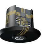
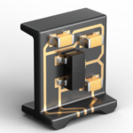
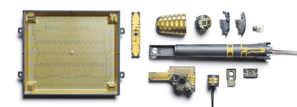
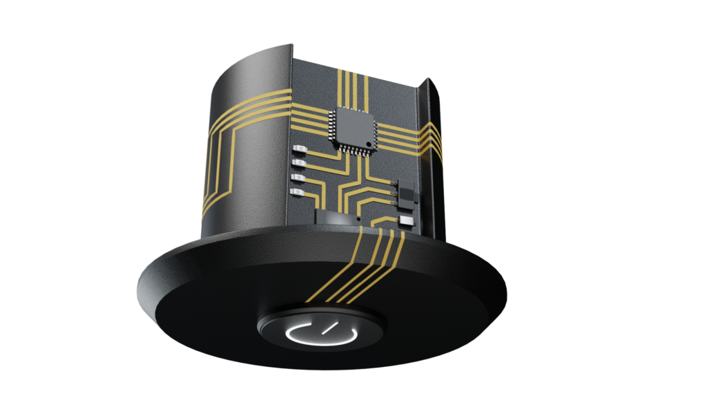
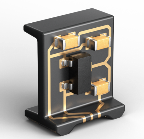
HARTING AG implements 3D-MID technology by applying conductive tracks three-dimensionally to components.
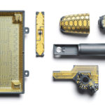
Applications of this technology (3D Circuits) include medical devices, computer, robotic, control and electromechanical systems.
It is ideal for series production of components with complex geometries and smallest space requirements.
3D-MID components are manufactured as follows:
The base body is manufactured by means of plastic injection molding. The raw material used contains special LDS additives that can be activated by laser.
With the LDS method (“Laser Direct Structuring”), which was developed by LPKF Laser & Electronics in 1996, the conductor track layout on the components is created with a laser beam. The conductor paths are then made conductive in a chemical coating process.
During plating, copper is deposited on the conductor track layout created by the laser. In this way, very precise electronic circuits are created.
The combination of mechanical and electronic components and the associated function integration makes the development and manufacture of complex electronic devices simpler and more cost-effective. Design-dependent devices such as in-ears or endoscope tips are made possible by this technology in the first place.
3D-Circuits technology opens up a world of new applications and potential savings for the manufacturer and therefore also for the consumer, through fewer production steps, shortened assembly times and smaller quantities of individual components.
Features and possibilities of HARTING’s 3D Circuits
- Combination and integration of mechanical and electronic functions in one component
- Miniaturization of components and modules
- Greatest possible design freedom
- Stable process chains and high quality standards – Swiss Made
- Weight reduction and associated very high sustainability
- Cost savings
3D-MID applications
3D-MID technology is a technological breakthrough in the design, development and production of existing and new products. Applications and technologies are for example:
- Medical equipment and instruments
- Diagnostic systems
- Sensor technology
- Imaging and monitoring systems
- Implants
- Micropumps and auto injectors
3D-MID in the medical world
HARTING 3D-MID technology offers great added value, especially to the medical world.
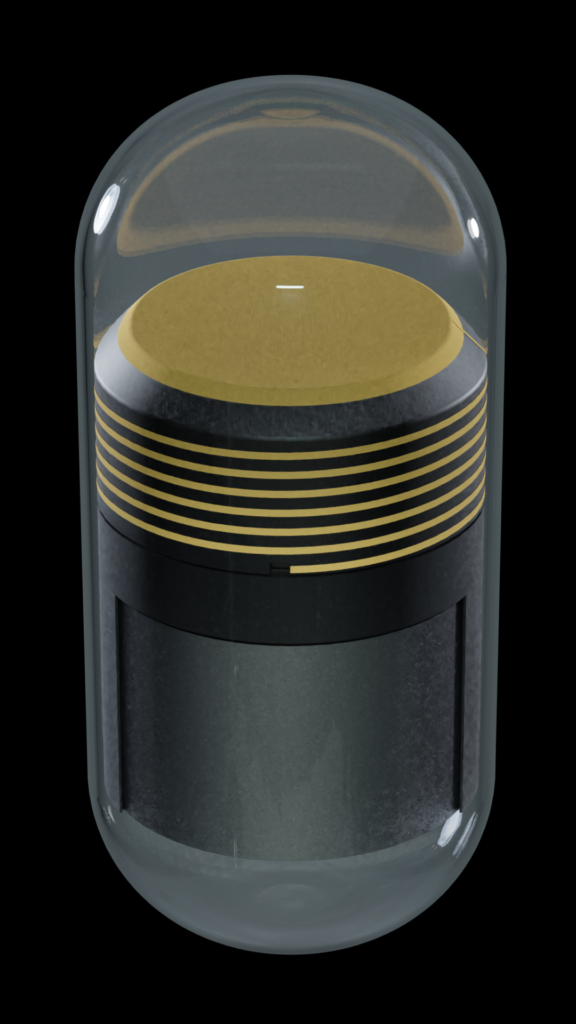
Many new developments in diagnostics and patient treatment have only been made possible by the miniaturization of electronics due to 3D-MID technology. For example, in the field of endoscopy, the miniaturization of LED and camera modules offers new possibilities.
And we go one step further.
The idea of being examined in one’s own body with a camera attached to a long, thin tube is often not considered particularly appealing.
With 3D Circuits technology, manufacturers can develop devices that are significantly more comfortable for patients, especially when it comes to intra-body examination, monitoring and diagnosis of the patient.
Instead of endoscopy, patients can now take a capsule, like a pill. This capsule contains a small camera that transmits 360-degree images so that, for example, the digestive tract can be examined.
3D-MID technology is also being used to develop new types of prostheses, such as the Luke Arm, a mind-controlled prosthetic arm that restores some functionality to patients who have lost limbs.
Smaller devices such as hearing aids, implants, and surgical and dental devices are also being redesigned using 3D-MID technology.
Outlook
The requirements for sustainability, communication and well-being are becoming ever higher in our modern world. Industry 4.0 or IoT are the current terms of choice here to describe these phenomena. Miniaturization and function integration can make a significant contribution here in product development to meet these requirements. And this is exactly the approach of the 3D-Circuits technology.