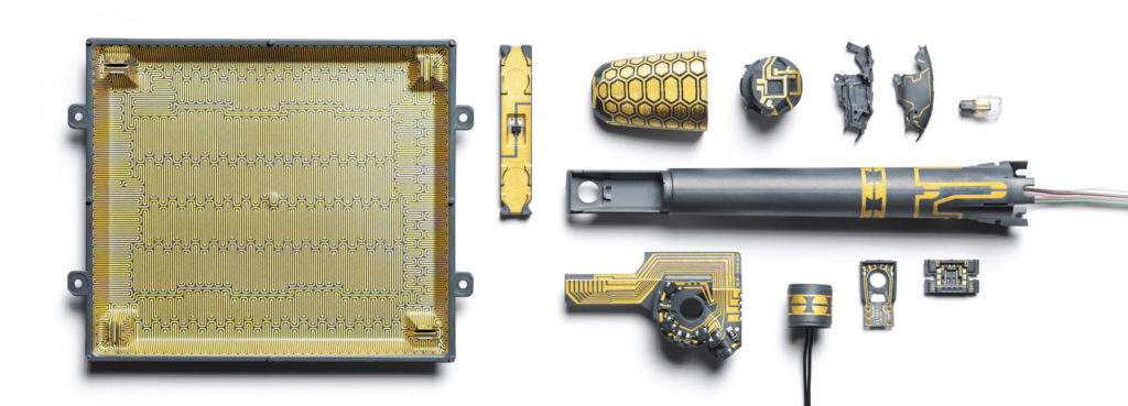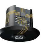
LDS enables the production of electronic assemblies with flexible geometric shapes. This process enables electronic products (such as smart phones, sensors or medical devices) to become even smaller and more powerful. Automated manufacturing processes also make this process more economically attractive.
There is less and less space available for electronic assemblies, so solutions are needed which replace conventional printed circuit boards. LDS enables further miniaturisation and makes increasingly complex geometric designs possible. This is a stable and reliable process that has established itself in quality-critical sectors such as medical technology or safety-relevant components for the automotive industry.
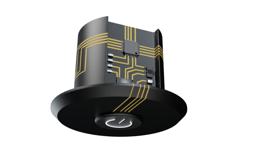
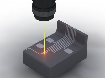
The LDS process enables three-dimensional assemblies
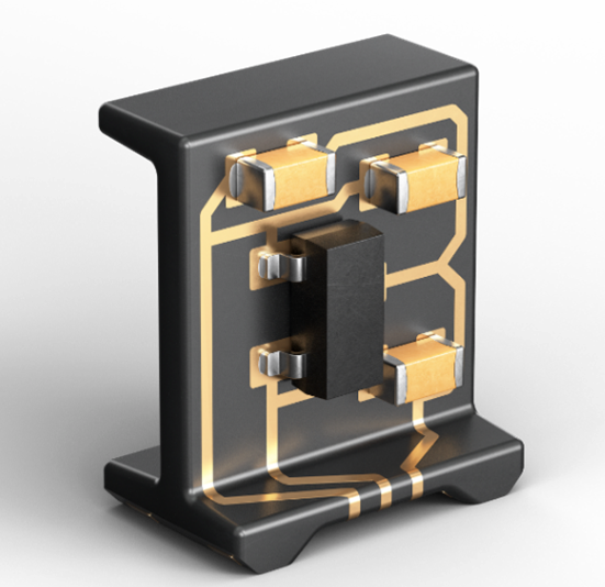
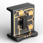
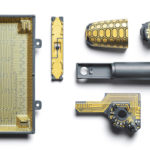
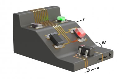
Direct laser structuring enables 3D-MID (Mechatronic Integrated Devices) assemblies to be produced. When using 3D-MID, electronic components can be fitted directly onto a three-dimensional base body, without circuit boards or connecting cables. The base body is manufactured using an injection moulding process, whereby the thermoplastic material has a non-conductive, inorganic additive.
The additives in the material are “activated” by direct laser structuring so that the plastic material can accommodate the electrical conductor paths. A laser beam writes the areas intended for the conductor paths and creates a micro-rough structure. The released metal particles form the nuclei for the subsequent chemical metallisation. In this way, the electrical conductor paths are applied to the areas marked by the laser. The other areas of the three-dimensional base body remain unchanged. The plastic component can then be assembled in standard SMD processes similar to a conventional PCB. It is also suitable for soldering in a reflow oven.
Versatile application of laser technology
HARTING 3D-MID AG is the largest supplier of 3D-MID components outside of Asia. HARTING uses highperformance laser systems for the LDS process, with three lasers working in parallel, each offset by 45 degrees. Thanks to an additional axis of rotation, components can be processed by the laser simultaneously from all sides (360 degrees). This technology enables flexible geometric shapes, such as reflector shells or LED lights, to be made. Despite the minimal conductor path thickness of 16 to 20 μm, the conductor paths are still suitable for demanding automotive components or for applications with currents up to 10 A – for example for heating coils in cameras which are used to prevent the optics from fogging up.
Frequent changes during the electronics development phase or new components with modified dimensions can lead to costly adjustments during conventional PCB production. The laser layout, in contrast, can be adapted very flexibly by using the parameters of the laser’s control software. No changes in the injection moulding are required for this.
The production of prototypes using LDS is also easier compared to conventional processes. HARTING can produce the plastic base body using LDS-compatible material and 3D printing. Injection moulding can also be used with inexpensive prototype tools.
New trends in the LDS process
Several aspects of LDS technology have been improved and further developed over the past few years.
- The working area of the laser has been enlarged from 160 x 160 x 80 mm to 200 mm x 200 mm x 80 mm, thus enabling a higher packing density and the processing of even larger components.
- The working speed of the laser can be doubled to 4 m/s by optimising the servo units and mirrors which guide the laser beam, thereby significantly reducing the processing time.
- The improvement of the optics enables the use of a laser with a diameter of 100 μm and a laser with a fine focus of 50 μm for processing even smaller structures.
HARTING is the only 3D-MID manufacturer in the world that has a laser system with three fine focus optics of 50 μm. Even smaller conductor path gaps can be achieved thanks to this fine focus laser. Thus, many conductor paths can be created on the same component and a higher packing density can be implemented. This is used for safety technology, among other things, because the closely spaced and intertwined conductors are capable of triggering safety alarms from even the smallest physical interference.
Advances in materials and economics
Only specially selected thermoplastics are certified for the LDS process; these are available from stock. The process can be further improved with customer-specific adjustments to the plastic material:
- HARTING uses a process which adds LDS additives to non-certified materials to make them MIDcompatible.
- Specific RAL or Pantone colours can be achieved with MID plastics by using colour pigments and special LDS additives.
- By selecting suitable additives, special RF characteristics can also be implemented, depending on the frequency range.
To further improve the cost-effectiveness of the manufacturing process, HARTING relies on automated robotic systems. The LDS laser system is equipped with a rotary indexing table so that a component can be inserted or removed while another component is still being processed. The in-feed and unloading procedures are automated by HARTING using robotics. This increases throughput and autonomy, while also enabling integration into automated production processes. An additional automation step is provided during the injection moulding process. Here, too, a robot takes over the removal of the injection moulded parts. The use of robotics also improves the precise reproducibility of the processes and, thus, overall product quality.
More growth for 3D-MID
HARTING reports increased demand for MID projects and has further expanded the 3D-MID division by investing in machinery and by acquiring a competitor’s business. Innovative in-house products are also contributing to further growth. HARTING has developed a solution based on 3D-MID technology which replaces flexible PCBs with a component carrier. Instead of using a flex-PCB, the component carrier can be fitted directly with electronic components, thus saving up to two thirds of the cost.
About HARTING 3D-MID
HARTING 3D-MID is offering the complete value chain for 3D-MID technologies from a single source, including development/prototyping of customer-specific products, injection moulding, laser direct structuring, metallisation, assembly and connection technology, as well as final inspection. Its core business is the production of mechatronic components for automobile manufacturing, industry, medical technology and sensor systems. HARTING is the largest supplier of 3D-MID components outside of Asia. HARTING 3D-MID is a business unit of the HARTING Technology Group, headquartered in Espelkamp, Germany.