As electronic devices continue to evolve and shrink, so do their circuits and, ultimately, their components. This development has raised the demand for component miniaturization. 3D-Circuits or also called 3D-MID (three-dimensional mechatronic integrated devices) makes this possible. It allows for more compact designs while enhancing functional density. In this article, we take a closer look at 3D-Circuits technology, what it is, its many benefits, its applications and a short overview about HARTING as a full-service provider.
The Miniaturization Revolution in Electronics
Smaller devices mean less environmental impact. A laptop, for example, uses 80% less power than a desktop computer, with a peak power consumption of 60 watts compared to 175 watts for desktops. This reduction in energy use is due to miniaturization.
Miniaturization has revolutionized many sectors, from medical and healthcare to automotive as well as industrial and consumer electronics. Here are a few drivers of this movement:
Aesthetic demands
We have come to expect our devices to be visually appealing and well-designed.
Portability
We also want our devices to be lightweight and easy to carry.
Cost savings
While miniaturization can be costly initially, it allows for the use of fewer materials, which can save money in the long run.
Eco-friendly power consumption reductions
Smaller parts consume less energy which helps lower operating costs, increase battery life, and promote greener products.
Less heat dissipation
Since smaller parts use less power, electronic devices generate less heat. This means bulky heatsinks or fans can be removed, reducing weight, cost, power, and noise.
Almost every industry is moving towards functional density, meaning that hardware components need to be interconnected and made smaller and smaller.
3D-MID is a way to fulfill those requirements by reducing mass and optimizing space while allowing for those parts to offer the same or more capabilities.
What Is 3D-MID?
The term “mechatronics” was coined in 1969 by a senior engineer of the Japanese firm Yaskawa. It is a combination of the words “Mecha” (machines) and “Tronics” (electronics).
Since then, the definition has evolved. It is now used to describe the abilities to use computers, electronics, and mechanics to build more intelligent systems, such as robotic, control, and electromechanical systems.
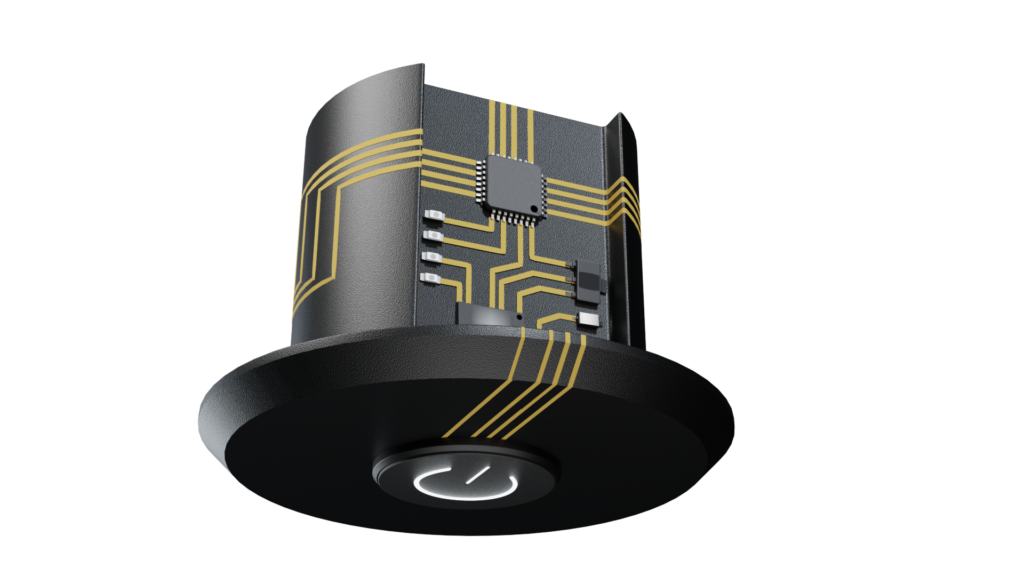
3D-MID stands for “Three Dimensional Moulded Interconnect Device” or “Three Dimensional Mechatronic Integrated Devices.” These are mechatronic devices that combine electronic and mechanical functionalities into a single three-dimensional component.
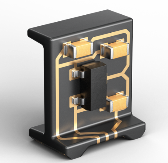
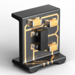
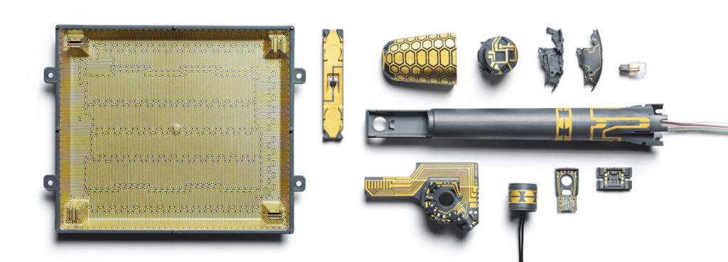
HARTING’s 3D-Circuits technology allows the 3D-MID parts or the injection-moulded thermoplastic part to be directly integrated with electronic circuits and components, making them more compact and functionally dense. Imagine a circuit board that is significantly smaller and composed of plastic rather than metal.
Furthermore, injection-moulded circuit boards significantly reduce the number of production processes, assembly times, individual components required, and therefore lowering the production costs.
How does 3D-Circuits technology work?
The flexibility of 3D-MID technology allows device designers to go where they need to. A three-dimensional component that combines electrical and mechanical functions allows for endless possibilities.
The designers lay down their requirements along with very specific measurements. The components are then constructed through injection moulding.
Injection moulding is when materials such as plastic are heated and melted before being injected into a mould and cooled to achieve the desired shape. It is a process often used by many industries because it enables the creation of parts with complex shapes quickly for mass production.
Because injection moulding is so flexible, designers can use it to construct virtually anything with the exact specifications. Before realising a mould, different forms of simulation can be used to check if the parts fulfill the requirements and sample parts from rapid prototyping can be made.
Next comes laser activation through laser-direct structuring (LDS), a procedure created by LPKF Laser & Electronics in 1996. It is where a laser beam defines the conductive trace, etching the layout directly into the injection-moulded plastic component.
The injection-moulded plastic will have special additives, which laser beams can detect. The lasers then reveal areas where the conductor structures will eventually be placed.
In the chemical plating process, copper only lays down on the laser structured areas. This allows the engineers to create very precise electronic circuits.
After metallization in a copper bath, conductive traces form in the areas that have been activated and will allow for metals to adhere to it.
Combining mechanical and electrical hardware makes designing and manufacturing electronic devices with complex functionality easier and less expensive. It essentially opens up a world of possibilities and possibly enormous savings for manufacturers and consumers.
What are the benefits and uses of 3D-MID technology?
- Integration of mechanical and electrical function into one component
- Better reliability and quality
- The flexibility allows for unlimited design options
- Helps reduce both size and weight
- Shortens assembly time and thus reduces manufacturing costs

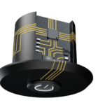
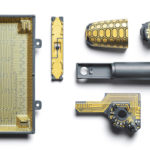
3D-MID Applications
Plastics and electronics come together in practically every piece of current and future technical equipment, from medical to automotive to consumer gadgets.
3D-MID technology is often regarded as the gamechanger in several applications such as:
- Sensor devices and miniaturized electronic packaging
- LED carriers and lighting modules
- Antennas and connectivity modules
Almost all industries can benefit from 3D-Circuits in some way as many sectors have significant needs for miniaturization, such as the medical field.
3D-MID in Medical market
Mechatronics is a promising discipline that benefits multiple industries, especially medical or healthcare.
Advancements in diagnostics and treatment have been made possible because of the miniaturization of electronics due to 3D-MID breakthroughs.
Imagine this: You need to have an endoscopy. Most people find the idea and the experience of having a long, thin tube with a small camera on the top go inside them uncomfortable.
But what if you were able to avoid that? Using 3D-MID, manufacturers can now design devices that are less invasive and more comfortable for patients, particularly when it comes to monitoring and examining the patient from the inside.
No longer is it necessary to insert a long endoscopic camera down the throat. You can instead consume a non-invasive capsule, similar to how you take your vitamins. This capsule contains a little endoscopic camera that transmits 360-degree pictures of your body to your doctor, allowing them to visualize your digestive tract without the need for invasive procedures.
This is just one example of how technological advancements can make a previously uncomfortable situation more pleasant.
Mechatronics is also being used to create new types of prosthetics, such as the Luke Arm, a mind-controlled arm prosthesis that gives patients who’ve lost limbs the ability to perform everyday tasks.
3D-MID technologies are also used to design smaller medical equipment such as hearing aids, implants, and surgical and dental devices. 3D-Circuits boards can be made in any size while maintaining the same functionality and safety standards.

This is a substitution for an endoscope. You basically swallow it like a pill which makes way more comfortable than an endoscope.
Conclusion
The possibilities with 3D-MID are unlimited. As this technology advances, we expect to see more organizations incorporate them for their space-saving projects, thereby reducing their assembly procedures and cutting costs.